Facilities

This lab equipped with several optical microscopes for basic sample observation and advance image recording.

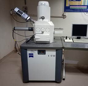
CARL ZEISS EVO 50 Tungsten SEM

Resolution: 2.0 nm @30 kV
Acceleration Voltage: 0.2 to 30 kV
Magnification: 5X to 10, 00, 000 X
Field of View: 8.5 mm at the analytical working distance (AWD)
Attachments: EDS & EBSD
X-ray Analysis: 8.5 mm AWD and 35° take-off angle
Detectors: SE in HV - Everhart - Thornley


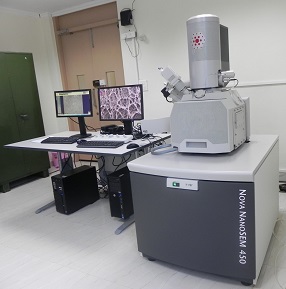
FEI NOVA NANO SEM 450 Field Emission SEM

Resolution: 1.0 nm @30 kV
Acceleration Voltage: 0.2 to 30 kV
Magnification: 5X to 10, 00, 000 X with HR/UHR mode
Field of View: 5.0 mm at the analytical working distance (AWD)
X-ray Analysis: 5.0 mm AWD and 35° take-off angle
Detectors:

  • In-lens SE detector (TLD-SE)
  • In-lens BSE detector (TLD-BSE)
  • Everhardt - Thornley SED
  • Low vacuum SED (LVD)
  • High sensitivity low kV directional backscattered detector (DBS)
  • BSD in all modes - quadrant semiconductor diode

Attachments: EDS & EBSD

EMITECH SC 7620 Sputter coater

Make: EMITECH
Type: Sputter coating Purpose: Conducting surface Coating Thickness: Few nm
Key Features:
Compact design
Simple operation
Glow discharge capability
Adjustable height specimen stage
Easy change sputter targets - Gold/Palladium (Au/Pd)

Recommended Materials: Non conducting materials